Tutorial
1. Graphical user interface
1.1 Overview of the software
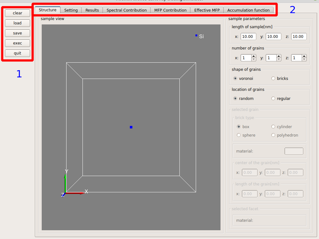
The first marker box shows the basic steps for the simulation.
clear: clear all configurations for current simulationload: load a existing simulationsave: save current configurationexec: run the simulationquit: exit the software
The second marker box shows main function tabs of the software.
The meaning of each tab will be explained later.
The workflow of the software:

We will describe the meaning of those tabs one by one the one in the following.
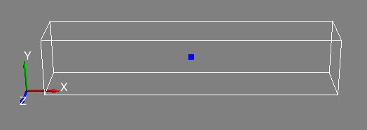
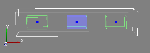
1.2 Structure
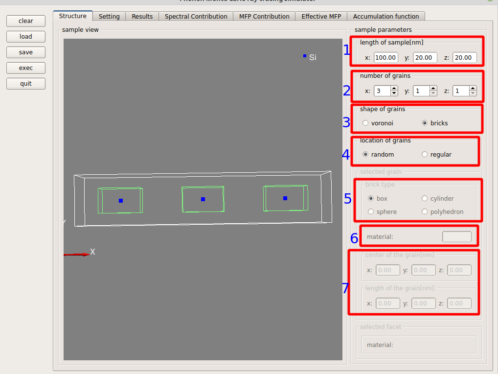
The meaning of each box is explained as follows:
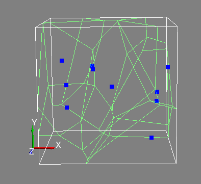
length of sample: set the dimensions of the simulation domainnumber of grains: number of grains in the nanostructureshape of grains: shape of each grain, which can be voronoi or bricks
Note
The shape vornoi means that the grains are generated from Voronoi diagram algorithm.
It is obtained by drawing perpendicular surfaces between randomly distributed points.
Note that for real case, the grain size is distributed in a log-normal manner.
We found that it has minor effect on the final thermal conductivity.
location of grains: set the location of each grain to be random or regular5.
brick type: set the shape of each bricks, which can be box, cylinder, sphere, or polyhedron. This setting is enabled when you click a grain. Note that if you set the grain to be polyhedron, a pop-up window will show up and allows you to specify the grain shape from aSTLfile. An example of usingSTLfile for simulation can be found here.
material: set the material of each grain.
Note
To select materials, we need to add it into the materials table first. A new material can be added to the material
table from Setting-> material table-> add material
center of grain: set the size of location of each grain. It is editable only when you have selected a grain in the structure.
1.3 Setting
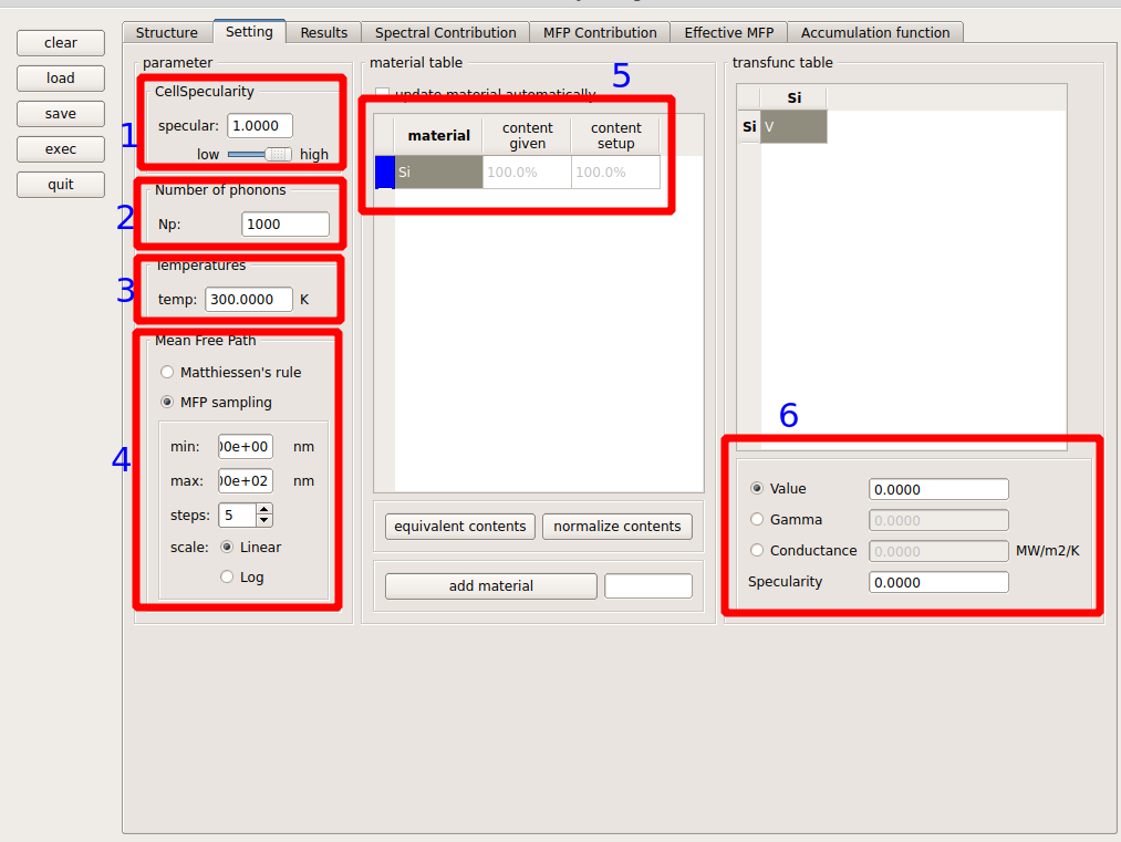
This figure shows the basic setting tabs of the software, the meaning of each marker box is explained as below:
CellSpecularity: set the specularity of the outermost surface of the simulation box
Tip
The default value for specularity is 1, which means that phonons will be specularly reflected by the outermost surface. It is useful for simulating of phonon transport in bulk system.
Number of phonons: set the number of phonons used to estimate the transmission. A recommended values is1000.Temperatures: set the simulation temperature.
Note
When the simulation temperature is different from the temperature used to calculate the bulk phonon properties, the temperature-dependent simulation is achieved by scaling the MFPs from empirical equations. To achieve better accuracy, we suggest to calculate the temperature bulk phonon properties from first principle calculation directly and use it as the input.
Mean Free Path: choose the mean free path (MFP) solver as well as the sampling range and points. We recommend to use theMatthiessen's rulemethod for the simulation.
Note
When click the MFP sampling, additional configuration box will pop-up and ask you to select the MFP sampling
range as well as the sampling points.
Note
In Matthiessen’s rule, the effective MFP is calculated by from formula:
where \(\Lambda_{bulk}\) is the bulk phonon MFPs that considered the phonon-phonon scattering. \(\Lambda_{bdy}\) is the MFP that due to boundary scattering.
For MFP sampling method, the phonon-phonon scattering is directly considered in the Monte Carlo ray tracing method without resorting to the above equation. To consider the phonon-phonon scattering, we assign a free path \(-\Lambda_{bulk} \mathrm{In}R\) to the particle, where R is a uniformly-distributed random number from 0 to 1. At the end of each free path, we assume that a phonon-phonon scatter has taken place and assign a new direction and a new free path to it.
material table: specify the matrix material. To add a new materials into the simulation, you first insert the name of the new material in theadd materialtext box and then click theadd materialto add.
Note
This table is used to specify the material of each grain, which is then used to specify the transmission and specularity at the surface. We should keep in mind, however, that it is not equivalent to read simulation with different grains.
transfunc table: specify thetransmissionand thespecularityparameter at the surface between two materials.
Note
The default value for transmission
is 0.5, which means that phonon have half-chances to transmit across the surface. This is a reasonable assumption
based on the diffuse mismatch model.
The default value for specularity is 0, means that phonon will be diffusively scattered after transmit/reflected at the surface.
That is, after hitting the surface, the phonon has no memory on the incident angle, and the reflected angle is chose
based on Lambert’s cosine law.
Warning
When simulating phonon transport in polycrystal materials, we should avoid using a transmission value of 0,
otherwise phonon cannot will be trapped into local region and cause fatal errors.
1.4 Thermal conductivity
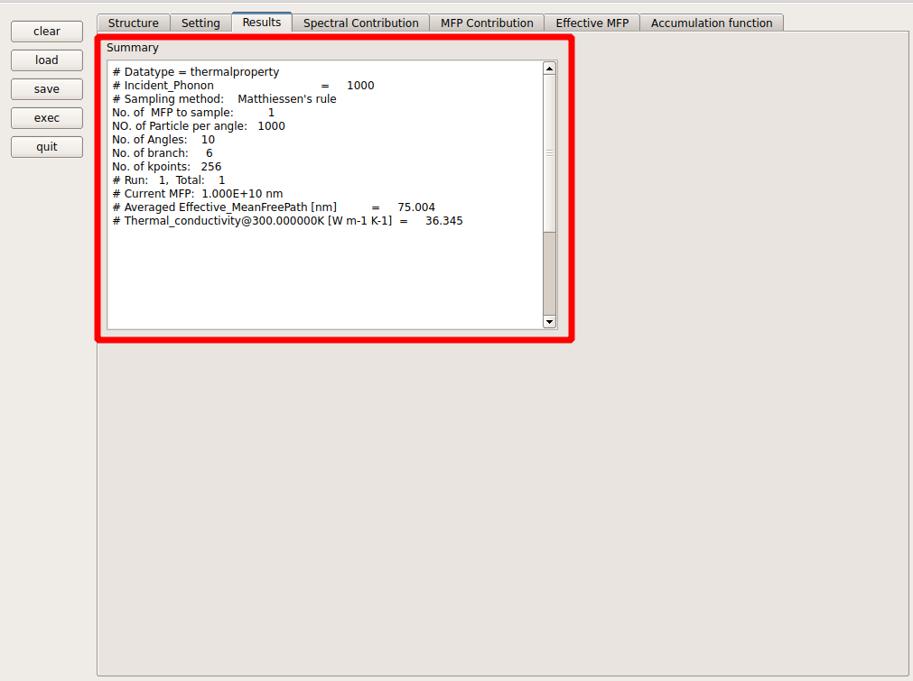
The main outputs when the simulation is done. The information in the output is self-explanatory.
In the text box we can see useful information like the averaged effective mean free path and the thermal conductivity of the nanostructure.
1.5 Spectral contribution
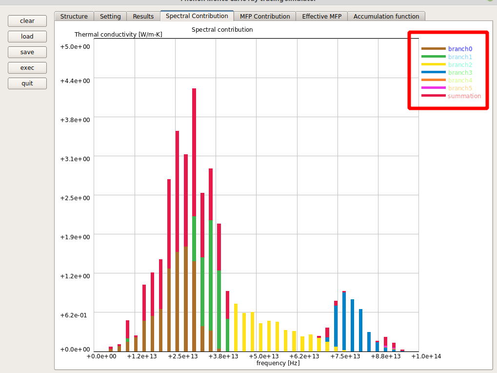
The spectral contribution of phonon at different frequency. Different colors represent the contributions from different phonon branch. By double click the legend on the marker box, you can display/hide the contribution from different branch.
This figure clearly shows the contribution of thermal conductivity from different phonon branch as well as its frequency range.
1.6 MFP contribution
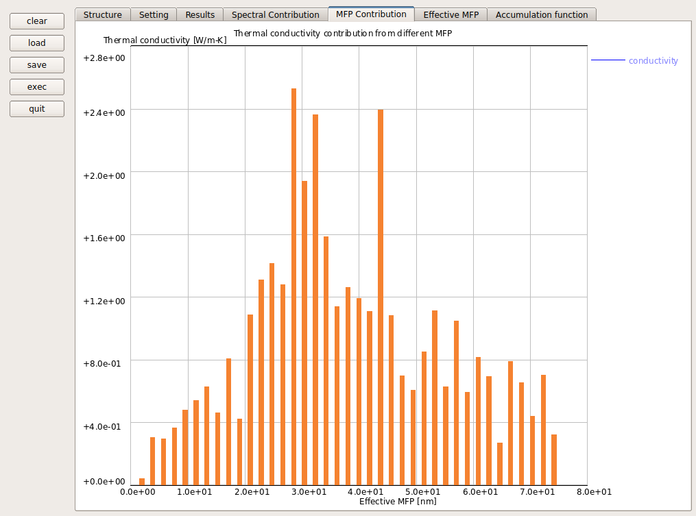
The contribution of thermal conductivity from phonon with different effective mean free paths. From this figure, we can see that in the nanostructure, the phonon with effective MFPs in the range of 10-70 nm have the dominate contribution to thermal conductivity.
Note
This simulation result suggest that we can inset nano-particles or interfaces with the characteristic length scale in this range to further scattered the dominate phonon and reduced the thermal conductivity.
1.7 Effective mean free path
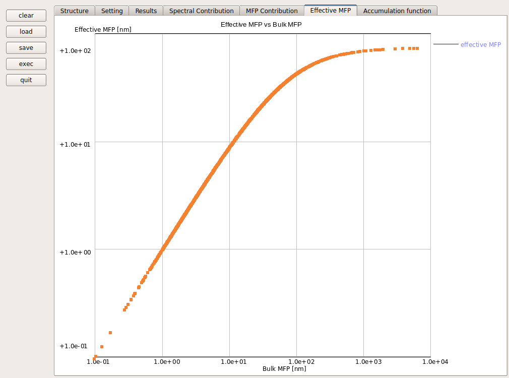
This figure shows the effective MFPs over the bulk MFPs in the nanostructure. We can see that the MFPs span a wide range of distribution (0.1 to 10000 nm). However, the effective MFPs distribution is reduced to a relative narrow distribution (0.1 to 100 nm) in the nanostructure due to the phonon surface scattering.
1.8 Accumulative function
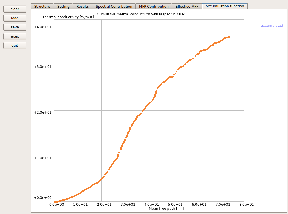
This figure shows the cumulative thermal conductivity with respect to the mean free path, which is another useful way to characterize the thermal properties of the nanostructure. For instance, we can see that phonons with effective MFPs less than 40 nm contribute 20 W/mK to the thermal conductivity.
2. Input files
Input files
## Monte Carlo
# parameters
temp # Temperature
    300.000000

## Ray tracing
# parameters
Np # number of incident phonons
    1000

# materials
Nm # number of materials
    1
material contents
    Si
            100.000000

# truns functions
Nt
    1 1
materials
    Si Si mode Value Specular
            1.000000 1.000000

# grains
Shape # shape of grains
    voronoi
Ng Ngx Ngy Ngz # number of grains
    1 1 1 1
## grain No.1
  generator
     +5.000000  +5.000000  +5.000000
  length
     +2.500000  +2.500000  +2.500000
  material
    Si
# facets of grain No.1
  Nf # number of facets
    6
#  facet No.1
  Nv # number of vertex
            4
    vertex 1
             +0.000000  +0.000000  +0.000000
    vertex 2
             +0.000000 +10.000000  +0.000000
    vertex 3
            +3000.000000 +10.000000  +0.000000
    vertex 4
            +3000.000000  +0.000000  +0.000000
  material_to = Boundary
  grain_to = 0
#  facet No.2
...
3. Outputs
If you are using the Linux version of the software, various outputs will also be dumped out to the terminal as well.
4. Examples
Note
All the examples shown here can be found from the Example folder in the software.
4.1 Silicon nanowire
The first example is to simulate the thermal transport in a nanowire.
Here the length of the nanowire is 100 nm and the cross-section is 20 nm x 20 nm.
Both of them can be modified easily from the Structure tab of the the software.
The surface specularity of the nanowire can be changed from the CellSpecularity box in the Setting tab.
The constituent material of the nanowire can be modified from the material table box in the Setting tab.
By default, the constituent material is silicon.
Here is the link to download the input file.
After the simulation, we can found that the thermal conductivity is 36 W/mK when the surface of nanowire is specular (specularity = 1), and it is reduced to 13.5 W/mK when the surface is diffusive (specularity = 0)
4.2 Nanowire with three grains
The second example is similar to the first one, but we added three grains into the structure.
The shape, location, and size of each grain can be configured from the Structure tab.
The phonon transmission and specularity parameter at each surface of the grain can be set from the transfunc table
in the Setting tab. Download
Note that if we set both the transmission and the specularity value to 1, it is equivalent to the say that the grain doesn’t exist at all. On the other hand, if we set the transmission to 0, the grain become to a empty hole.
Here the results we have got. The specularity at the out-most surface is 0.
Transmission |
Specularity |
Thermal conductivity [W/mK] |
|---|---|---|
0 |
0 |
8.5 |
0 |
0.5 |
8.7 |
0 |
1 |
9.3 |
0.5 |
0.5 |
11.4 |
1 |
0.5 |
13.0 |
1 |
1 |
13.8 |
4.3 Polycrystal Si
In the third example, we investigate thermal transport in polycrystal silicon. The dimension of the structure is
100nm x 100nm x 100nm and it contains 10 grains. Download
Transmission |
Specularity |
Thermal conductivity [W/mK] |
|---|---|---|
0.5 |
0 |
14.8 |
0.5 |
0.5 |
16.0 |
0.5 |
1 |
17.6 |
1 |
0 |
20.1 |
1 |
0.5 |
22.9 |
1 |
1 |
25.8 |
4.4. Rough nanowire
In this example, we study thermal transport in a rough nanowire, the structure of the rough surface is generated from
CAD software and it saved in a STL format. The CAD file can be downloaded from here.
The input file for the simulation can be found here
4.5 Diamond thinfilm
In the last example, we investigate the thermal transport in diamond thin film. The input file can be found here.
The thermal conductivity of diamond thinfilm at various thickness is shown in the figure below.
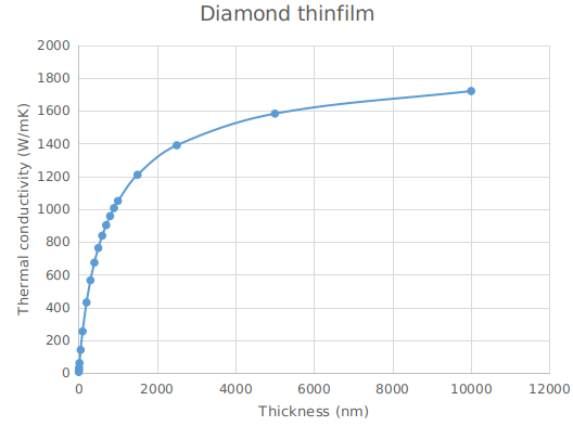
We can see that the thermal conductivity increases with the film thickness, and only shows signature of convergence at film thickness larger than 10 um. The simulation results suggest the existence phonons mode with extreme large mean free paths in diamond.
5. Benchmark simulations
5.1 Thermal conductivity of nanowire
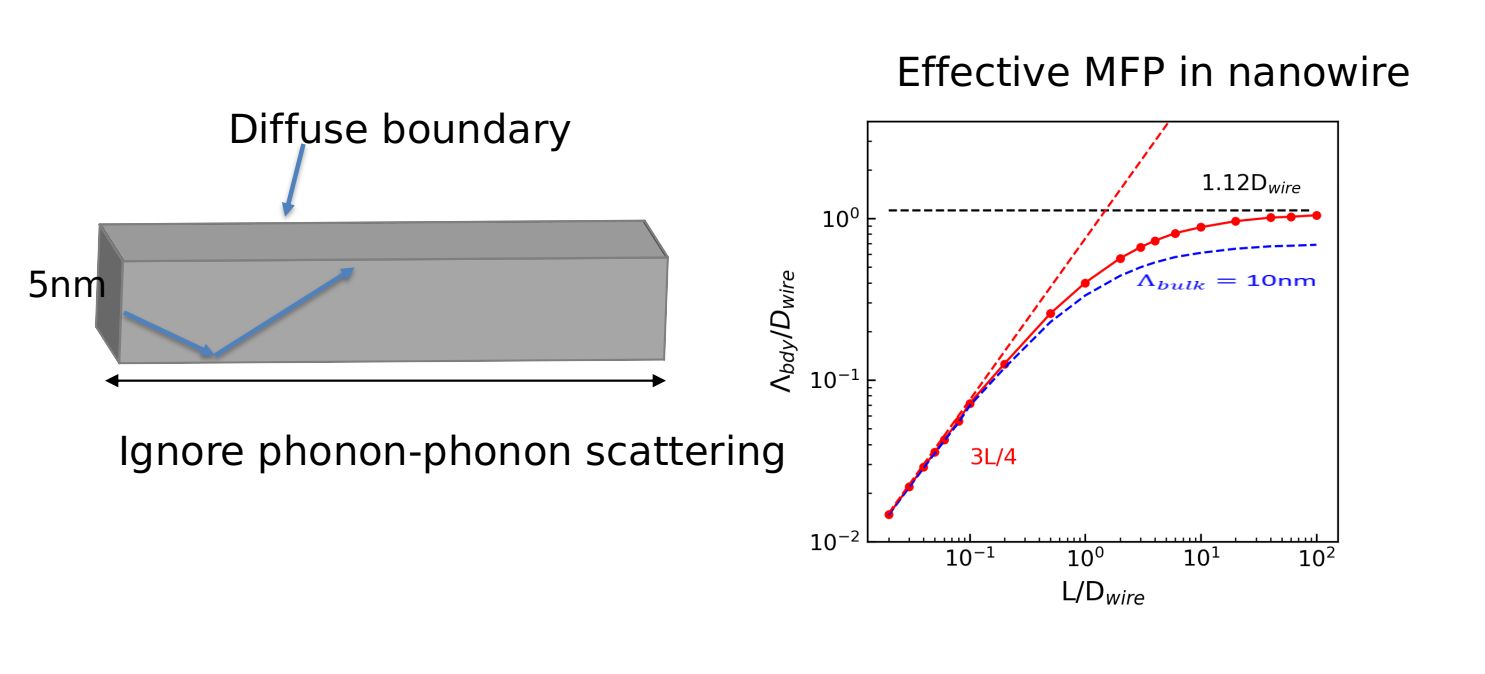
First we validate our software by studying the thermal conductivity in a square nanowire, as it is a well-studied system with analytical solutions. In the long length limit, we have \(\Lambda_{bdy} = 1.12D_{wire}\); while in the short length limit, the MFP is independent on the width of the nanowire and reads as \(\Lambda_{bdy} = 3L/4\). From the above figure, we can see that the simulated effective MFPs matched well the these two limits. In addition, the simulations also provides results at intermediate region, for which the analytical results is unavailable.
5.2 Matthiessen’s rule vs. MFP sampling
Here is a comparison between between the Matthiessen’s rule and the MFP sampling methods. The input file used for the
simulation can be found here.
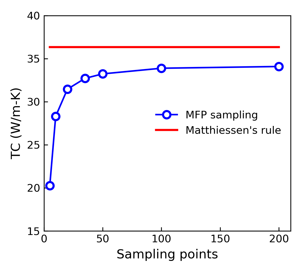
We can see that for MFP sampling method, the simulating results will reach a converged value when the number of the sampling points is
larger than 50. The prediction from the MFP sampling method is slightly lower than that from the Matthiessen’s rule. The
difference is about 5 percent.
Moreover, the simulation time used in MFP sampling method is about 1-2 orders of magnitude larger than that used in the
Matthiessen’s rule, depending on the number of sampling points.
Therefore, we suggest to use the Matthiessen's rule for the simulation as much as possible.
Note
The Matthiessen’s rule will work well when the different scattering channels are independent with each other. This is the case for structures like thin films or nanowires. However, for other structures like nano-porous materials, the internal scattering at porous edges could be strong direction dependent and coupled with the scattering at free surface. For this case, The MFP sampling method may give a better result.